- 您现在的位置:买卖IC网 > Sheet目录1993 > DS1243Y-120 (Maxim Integrated Products)IC NVSRAM 64KBIT 120NS 28DIP
DS1243Y
7 of 14
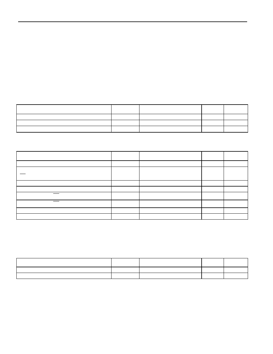
ABSOLUTE MAXIMUM RATINGS
Voltage Range on Any Pin Relative to Ground……………………………………………..-0.3V to +6.0V
Operating Temperature Range……………………………………………...0°C to +70°C (noncondensing)
Storage Temperature Range……………………………………………...-40°C to +85°C (noncondensing)
Lead Temperature (soldering, 10s)……… . . . . . . . . . . . . . . . . . . . . . . . . . . . . . . . . . . . . . . . . . . . +260°C
Note: EDIP is wave or hand-soldered only.
This is a stress rating only and functional operation of the device at these or any other conditions above those indicated in the operation
sections of this specification is not implied. Exposure to absolute maximum rating conditions for extended periods of time may affect
reliability.
RECOMMENDED OPERATING CONDITIONS
(TA = 0°C to +70°C)
PARAMETER
SYMBOL
MIN
TYP
MAX
UNITS
NOTES
Power Supply Voltage
VCC
4.5
5.0
5.5
V
Input Logic 1
VIH
2.2
VCC+0.3
V
Input Logic 0
VIL
-0.3
+0.8
V
DC ELECTRICAL CHARACTERISTICS
(VCC = 5V ±10%, TA = 0°C to +70°C.)
PARAMETER
SYMBOL
MIN
TYP
MAX
UNITS
NOTES
Input Leakage Current
IIL
-1.0
+1.0
A
12
I/O Leakage Current
CE ≥
VIH ≤ VCC
IIO
-1.0
+1.0
A
Output Current @ 2.4V
IOH
-1.0
mA
Output Current @ 0.4V
IOL
2.0
mA
Standby Current CE = 2.2
ICCS1
5.0
10
mA
Standby Current CE = VCC – 0.5V
ICCS2
3.0
5.0
mA
Operating Current tCYC = 200ns
ICC01
85
mA
Write Protection Voltage
VTP
4.25
4.5
V
DC TEST CONDITIONS
Outputs are open; all voltages are referenced to ground.
CAPACITANCE
(TA = +25°C)
PARAMETER
SYMBOL
MIN
TYP
MAX
UNITS
NOTES
Input Capacitance
CIN
5
10
pF
Input/Output Capacitance
CI/O
5
10
pF
发布紧急采购,3分钟左右您将得到回复。
相关PDF资料
DS1244W-120IND
IC NVSRAM 256KBIT 120NS 28DIP
DS1248Y-70IND
IC NVSRAM 1MBIT 70NS 32DIP
DS1251WP-120+C02
IC NVSRAM 34PWRCP
DS1254WB-150
IC NVSRAM 16MBIT 150NS 168BGA
DS1286I+
IC TIMEKEEPER WATCHDOG 28-EDIP
DS12885T
IC RTC W/RAM 128 BYTE 32-TQFP
DS12C887A+
IC RTC W/RAM 128 BYTE 24-EDIP
DS12CR887-5+
IC RTC W/RAM 128 BYTE 24-EDIP
相关代理商/技术参数
DS1243Y120+
制造商:Maxim Integrated Products 功能描述:
DS1243Y-120+
功能描述:实时时钟 64k NV SRAM w/Phantom Clock RoHS:否 制造商:Microchip Technology 功能:Clock, Calendar. Alarm RTC 总线接口:I2C 日期格式:DW:DM:M:Y 时间格式:HH:MM:SS RTC 存储容量:64 B 电源电压-最大:5.5 V 电源电压-最小:1.8 V 最大工作温度:+ 85 C 最小工作温度: 安装风格:Through Hole 封装 / 箱体:PDIP-8 封装:Tube
DS1243Y-120+
制造商:Maxim Integrated Products 功能描述:IC
DS1243Y-150
制造商:DALLAS 制造商全称:Dallas Semiconductor 功能描述:64K NV SRAM with Phantom Clock
DS1243Y4120
制造商:Maxim Integrated Products 功能描述:
DS-1243ZJ
制造商:Hikvision USA 功能描述:DOME CAMERA PENDANT MOUNT14.3IN X 7.3 X 7.2IN 制造商:HIKVISION 功能描述:DOME CAMERA PENDANT MOUNT 14.3IN X 7.3 X 7.2IN
DS1244
制造商:BB 制造商全称:BB 功能描述:Low-Power, 24-Bit ANALOG-TO-DIGITAL CONVERTER
DS1244P
制造商:DALLAS 制造商全称:Dallas Semiconductor 功能描述:256k NV SRAM with Phantom Clock